PCIe Study Notes
The Credit Goes To
A Practical Tutorial on PCIe for Total Beginners on Windows (Part 1)
PCIe Study Notes
ACPI x64-based PC
PCIe bus is not the initial layout of the system presented by firmware during boot. ACPI (Advanced Configuration & Power Interface) is what describes the existence of PCIe to the OS.
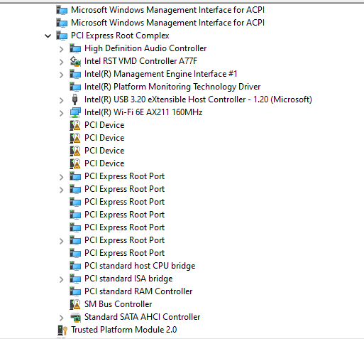
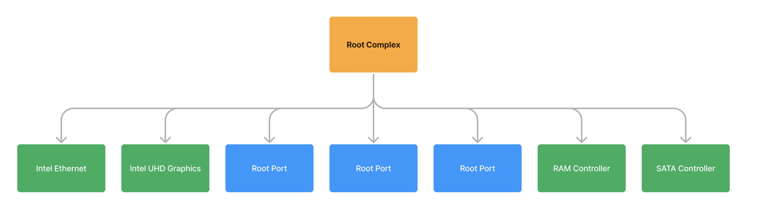
PCIe Tree Root Complex
#rootcomplex
The PCI Express Root Complex
PCI Express Root Port
Similar to a port on motherboard A port that another PCIe Endpoint or PCIe Switch can be connected to.
- An Endpoint ( a physical device - Type 0)
- configured as a device to talk to
- A Switch (a Bridge device - Type 1)
- other is configured as a device to route packets
- Root Complex Integrated Endpoints (RCIE, Marked in Green below) since they are intergrated directly on the Root Complex
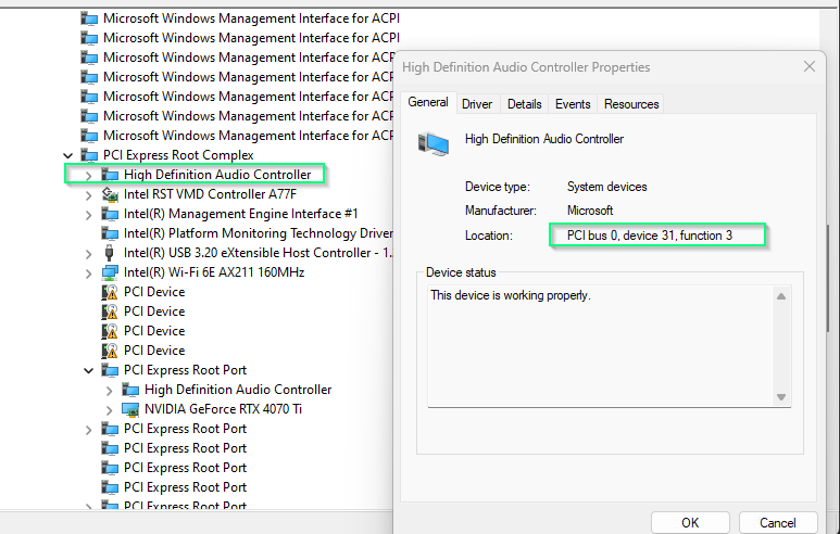
Bus/Device/Function
Bus
#bdf
- All busses on the system are identified with a number (0-255)
- Bus/Device/Function identifies where in the PCIe hierarchy the device is located so we can communicate with it.
- Bus “0” lcoated on the silicon of the CPU*
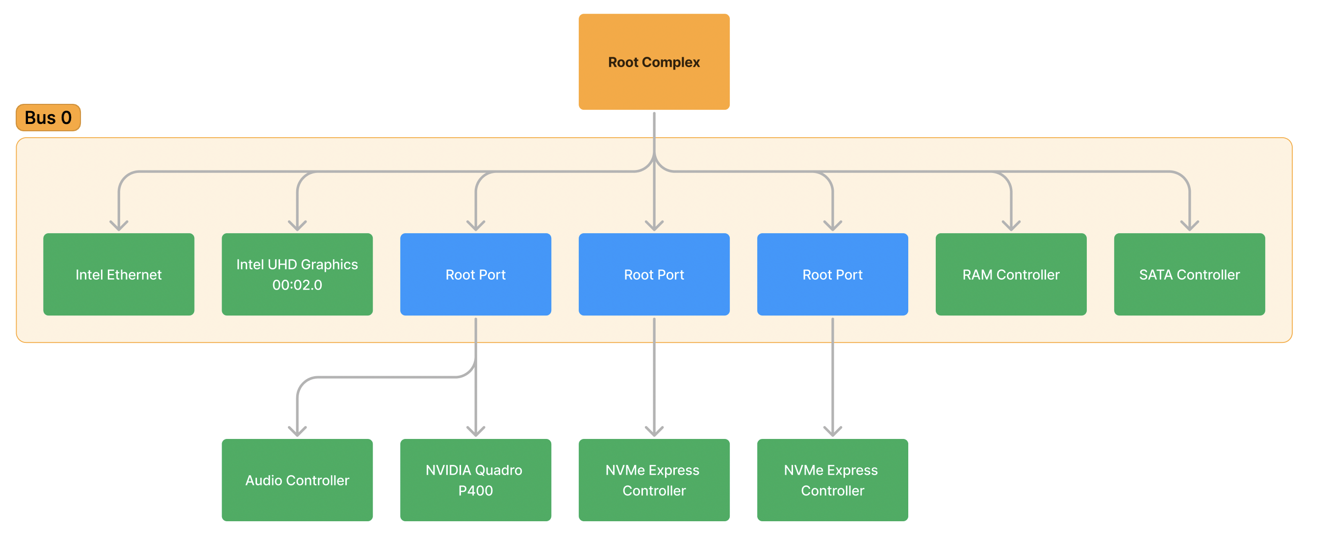 Ex. Bus 0
 Ex. Bus 1 (under a Root )
Device
- Device ID represents a physical device
Function
- Function ID represents the distinct capablity the physical device supports and expose to the system
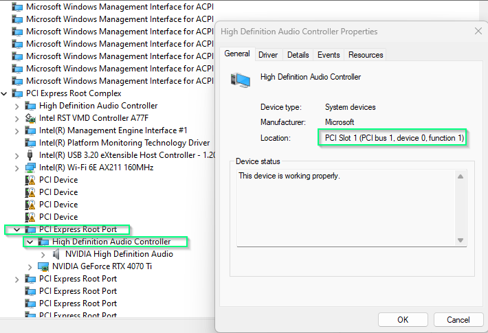
- A device that exposes more than one function is a Multi-Function Device (MFD)* - More PCI connections (e.x., NVIDIA GEFORCE RTX 4070TI and NVIDIA HIGH DEFINITION AUDIO devices)
Configuration Space
- A section of memory on the system which allows the kernel to enumerate, query info, and setup PCI devices
Capabilities
- In Configuration Space, Capabilities section details features a device is capable of
- Any new feature will be added to this list
-
WinDbg KD
1
2
3
4
5
6
7
8
9
10
11
12
13
14
15
16
17
18
19
20
21
22
23
24
25
26
27
28
29
30
31
32
33
34
35
36
37
38
kd> !pcitree
Bus 0x0 (FDO Ext ffffdc89b9f75920)
  (d=0,  f=0) 80866f00 devext 0xffffdc89b0759270 devstack 0xffffdc89b0759120 0600 Bridge/HOST to PCI
  (d=1,  f=0) 80866f02 devext 0xffffdc89ba0c74c0 devstack 0xffffdc89ba0c7370 0604 Bridge/PCI to PCI
  Bus 0x1 (FDO Ext ffffdc89ba0aa190)
    No devices have been enumerated on this bus.
  (d=2,  f=0) 80866f04 devext 0xffffdc89ba0c94c0 devstack 0xffffdc89ba0c9370 0604 Bridge/PCI to PCI
  Bus 0x2 (FDO Ext ffffdc89ba0a8190)
    (d=0,  f=0) 10de13bb devext 0xffffdc89ba04f270 devstack 0xffffdc89ba04f120 0300 Display Controller/VGA
    (d=0,  f=1) 10de0fbc devext 0xffffdc89ba051270 devstack 0xffffdc89ba051120 0403 Multimedia Device/Unknown Sub Class
  (d=3,  f=0) 80866f08 devext 0xffffdc89ba0cb4c0 devstack 0xffffdc89ba0cb370 0604 Bridge/PCI to PCI
  Bus 0x3 (FDO Ext ffffdc89ba08f190)
    No devices have been enumerated on this bus.
  (d=5,  f=0) 80866f28 devext 0xffffdc89ba0cd4c0 devstack 0xffffdc89ba0cd370 0880 Base System Device/'Other' base system device
  (d=5,  f=1) 80866f29 devext 0xffffdc89ba0cf4c0 devstack 0xffffdc89ba0cf370 0880 Base System Device/'Other' base system device
  (d=5,  f=2) 80866f2a devext 0xffffdc89ba0d14c0 devstack 0xffffdc89ba0d1370 0880 Base System Device/'Other' base system device
  (d=5,  f=4) 80866f2c devext 0xffffdc89ba0d34c0 devstack 0xffffdc89ba0d3370 0800 Base System Device/Interrupt Controller
  (d=11, f=0) 80868d7c devext 0xffffdc89ba0d84c0 devstack 0xffffdc89ba0d8370 ff00 (Explicitly) Undefined/Unknown Sub Class
  (d=11, f=4) 80868d62 devext 0xffffdc89ba0da4c0 devstack 0xffffdc89ba0da370 0106 Mass Storage Controller/Unknown Sub Class
  (d=14, f=0) 80868d31 devext 0xffffdc89ba0dc4c0 devstack 0xffffdc89ba0dc370 0c03 Serial Bus Controller/USB
  (d=16, f=0) 80868d3a devext 0xffffdc89ba0de4c0 devstack 0xffffdc89ba0de370 0780 Simple Serial Communications Controller/'Other'
  (d=16, f=3) 80868d3d devext 0xffffdc89ba0e04c0 devstack 0xffffdc89ba0e0370 0700 Simple Serial Communications Controller/Serial Port
  (d=19, f=0) 808615a0 devext 0xffffdc89ba0e24c0 devstack 0xffffdc89ba0e2370 0200 Network Controller/Ethernet
  (d=1a, f=0) 80868d2d devext 0xffffdc89ba0e44c0 devstack 0xffffdc89ba0e4370 0c03 Serial Bus Controller/USB
  (d=1b, f=0) 80868d20 devext 0xffffdc89ba0254c0 devstack 0xffffdc89ba025370 0403 Multimedia Device/Unknown Sub Class
  (d=1c, f=0) 80868d10 devext 0xffffdc89ba0274c0 devstack 0xffffdc89ba027370 0604 Bridge/PCI to PCI
  Bus 0x4 (FDO Ext ffffdc89ba0a9190)
    No devices have been enumerated on this bus.
  (d=1c, f=1) 80868d12 devext 0xffffdc89ba02c4c0 devstack 0xffffdc89ba02c370 0604 Bridge/PCI to PCI
  Bus 0x5 (FDO Ext ffffdc89b9fe6190)
    No devices have been enumerated on this bus.
  (d=1c, f=3) 80868d16 devext 0xffffdc89ba02e4c0 devstack 0xffffdc89ba02e370 0604 Bridge/PCI to PCI
  Bus 0x6 (FDO Ext ffffdc89ba0a7190)
    (d=0,  f=0) 12838893 devext 0xffffdc89ba062270 devstack 0xffffdc89ba062120 0604 Bridge/PCI to PCI
    Bus 0x7 (FDO Ext ffffdc89ba064250)
      No devices have been enumerated on this bus.
  (d=1c, f=4) 80868d18 devext 0xffffdc89ba0304c0 devstack 0xffffdc89ba030370 0604 Bridge/PCI to PCI
  Bus 0x8 (FDO Ext ffffdc89ba0b2190)
Device Detail
1
2
3
4
5
6
7
8
9
10
11
12
13
14
15
16
17
18
19
20
21
22
23
24
25
26
27
28
29
30
!devext 0xffffdc89ba04f270
PDO Extension, Bus 0x2, Device 0, Function 0.
  DevObj 0xffffdc89ba04f120  Parent FDO DevExt 0xffffdc89ba0a8190
  Device State = PciStarted
  Vendor ID 10de (NVIDIA CORPORATION)  Device ID 13BB
  Subsystem Vendor ID 103c (HEWLETT-PACKARD COMPANY)  Subsystem ID 1098
  Header Type 0, Class Base/Sub 03/00  (Display Controller/VGA)
  Programming Interface: 00, Revision: a2, IntPin: 01, RawLine 00
  Possible Decodes ((cmd & 7) = 7): BMI
  Capabilities: Ptr=60, power msi express
  Express capabilities: (BIOS controlled)
  Logical Device Power State: D0
  Device Wake Level:          Unspecified
  WaitWakeIrp:                <none>
  Requirements:     Alignment Length    Minimum          Maximum
    BAR0    Mem:    01000000  01000000  0000000000000000 00000000ffffffff
    BAR1    Mem:    10000000  10000000  0000000000000000 ffffffffffffffff
    BAR3    Mem:    02000000  02000000  0000000000000000 ffffffffffffffff
    BAR5     Io:    00000080  00000080  0000000000000000 00000000ffffffff
      ROM BAR:      00080000  00080000  0000000000000000 00000000ffffffff
    VF BAR0 Mem:    00080000  00080000  0000000000000000 00000000ffffffff
  Resources:        Start            Length
    BAR0    Mem:    00000000f2000000 01000000
    BAR1    Mem:    00000000e0000000 10000000
    BAR3    Mem:    00000000f0000000 02000000
    BAR5     Io:    0000000000001000 00000080
  Interrupt Requirement:
    Line Based - Min Vector = 0x0, Max Vector = 0xffffffff
    Message Based: Type - Msi, 0x1 messages requested
  Interrupt Resource:    Type - MSI, 0x1 Messages Granted
Communication Between Software and PCI Devices
- Through “Memory read and writes”
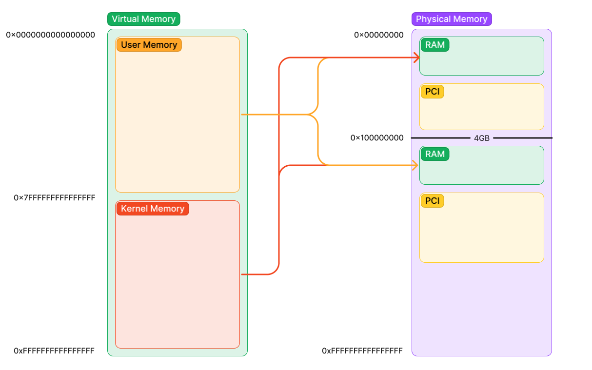
Type of Physical Memory
- RAM - read and write retrieved from DRAM DIMMs
- Device Memory - When reads and writes to, talk to devices on system. Doesn’t store memory on the device. It all happens within Device Register that configures the inner workings of the device (MMIO)
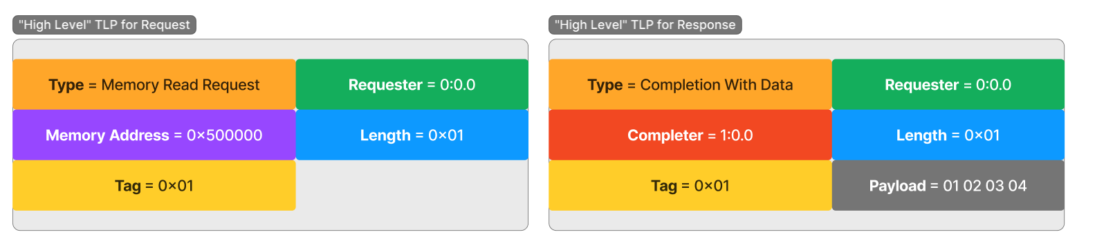
Transmission-Layer Packet
- When a read/writes happens in Device Memory, TLP was generated by CPU and on Root Complex and forwarded to device
- The kernel must ask the memory manager to map this physical memory into a virtual address. Then, software instructions can use the virtual address of the mapping to read and write from physical addresses. Do ne by
pci.sys, partially byacpi.sys, and partially by the kernel (specifically the HAL).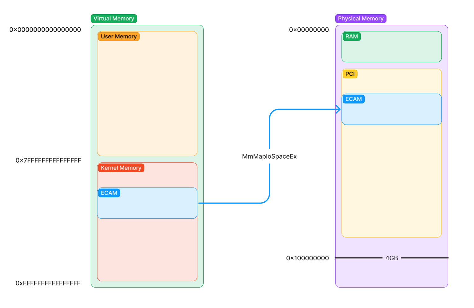
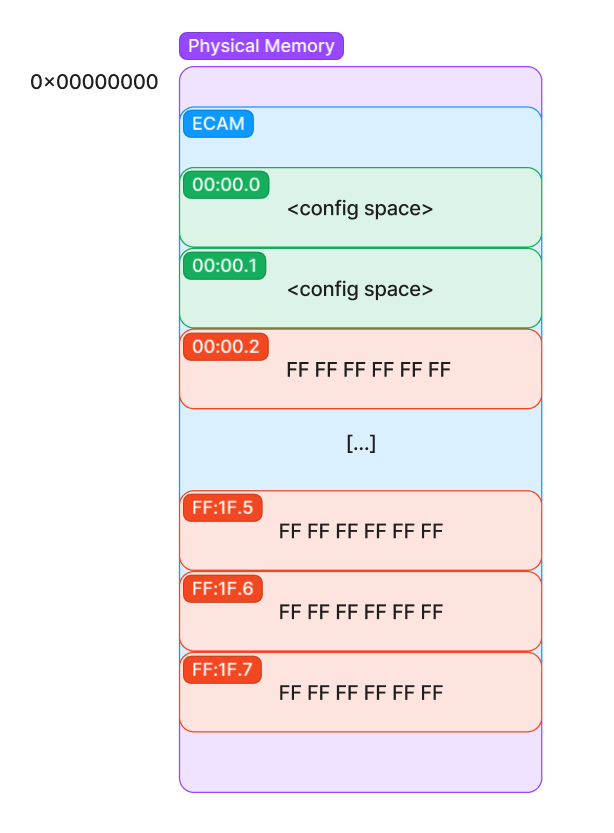
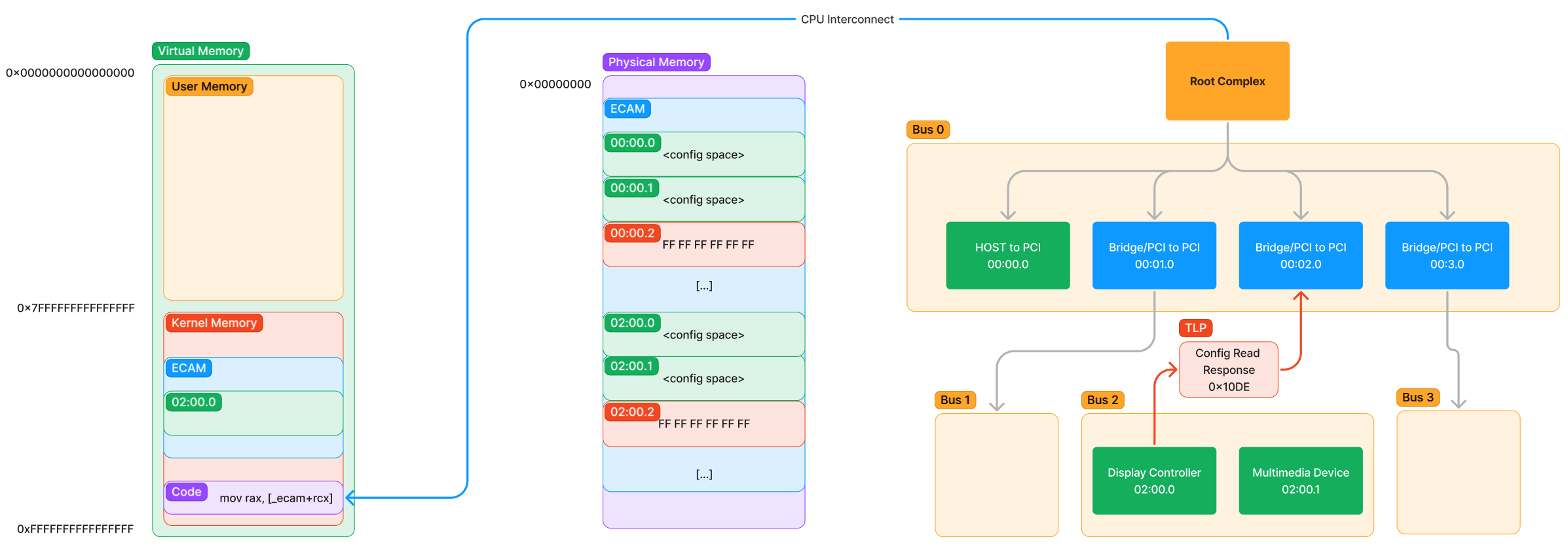
Configuration Space is located in Extended Configuration Access Management (ECAM) /PCI regions are located is platform dependent. Firmware at boot time will assign all special regions of physical memory of the system and communicate it to the OS
Accessing
- Map the physical memory into virtual memory (RAM)
- Enumerate the ECAM to identify functions exist in the device
- Physical address is read, CPU Interconnect to inform Root Complex of the access
- Root Complex generates a TLP and sends it
- Received by the device and responds
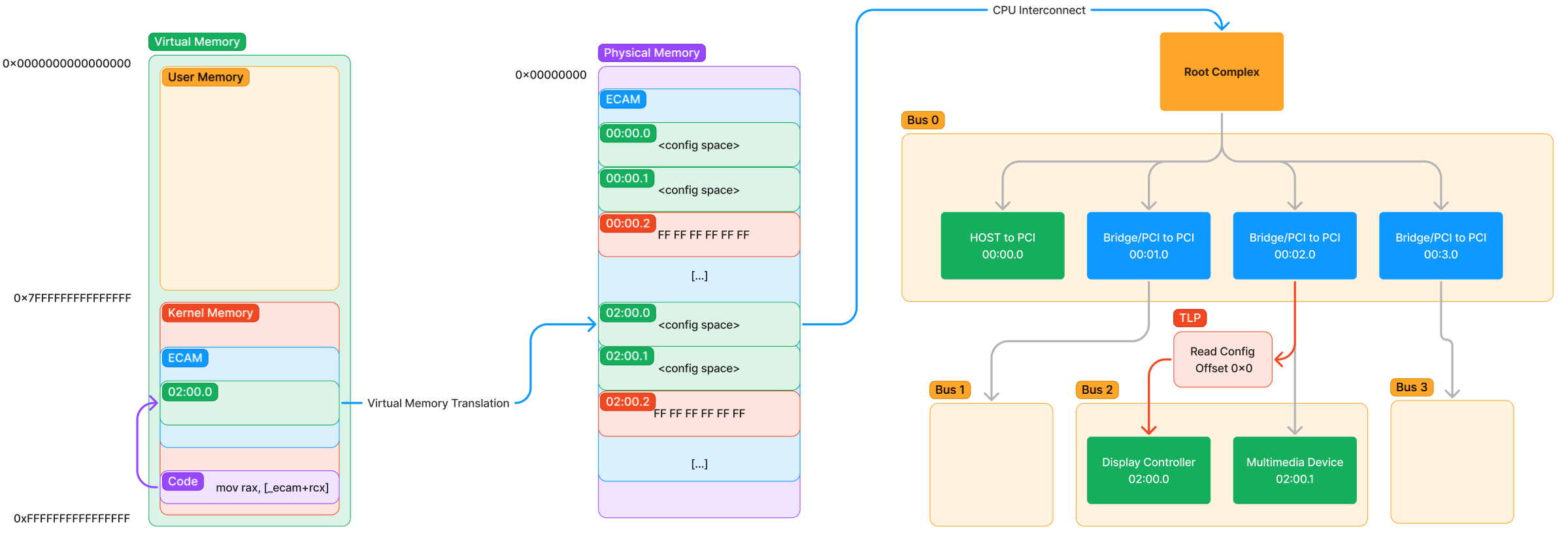
- Response goes to Root Complex informs CPU. Slow downs the process alot (that’s why there’s Direct Memory Access (DMA))
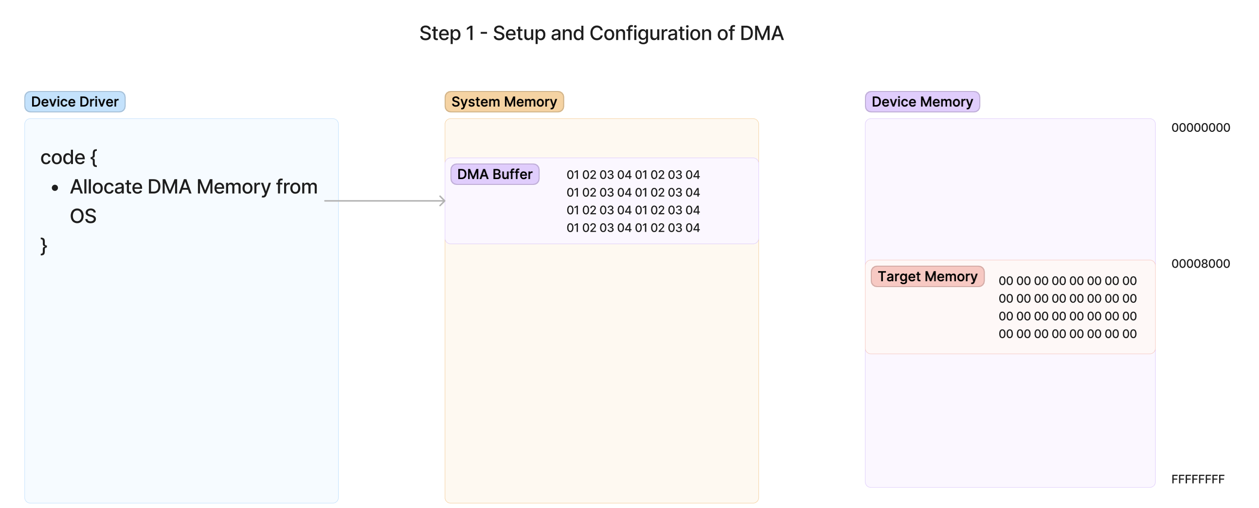
DMA Transcation
Step 1 - Allocating DMA Memory from the OS
- Setup System RAM for read-write memory pages
- Either IOMMU Remapping. or contiguous physical memory
- device logical address , the memory device can see and use in the system RAM
Step 2 - Programming DMA addresses to the device and beginning transfer
- driver should program the device is to either refer to its general standard such as the NVMe Specification or to simply work with the hardware designer
- Simple communication below :
- Driver communicate the DMA memory address to the device by writing the addresses to BAR0 mapping
!
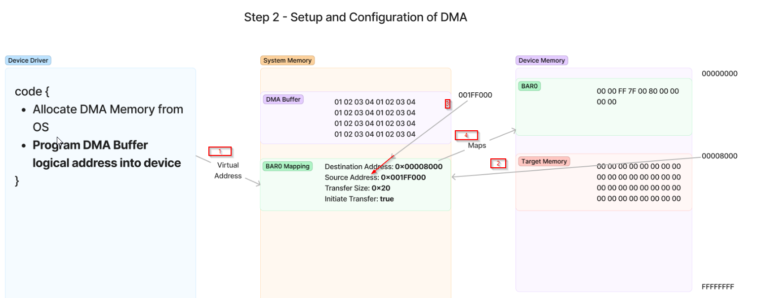
- Driver communicate the DMA memory address to the device by writing the addresses to BAR0 mapping
!
Step 3 - Device performs DMA transaction
#dmaengine
- After the DMA source/destination buffer has been configured on the device end, DMA Engine takes over
- DMA Engine will read those configuration at BAR0 and start handling/generating TLPs
- The Memory Address used to detemine which device is being requested for access
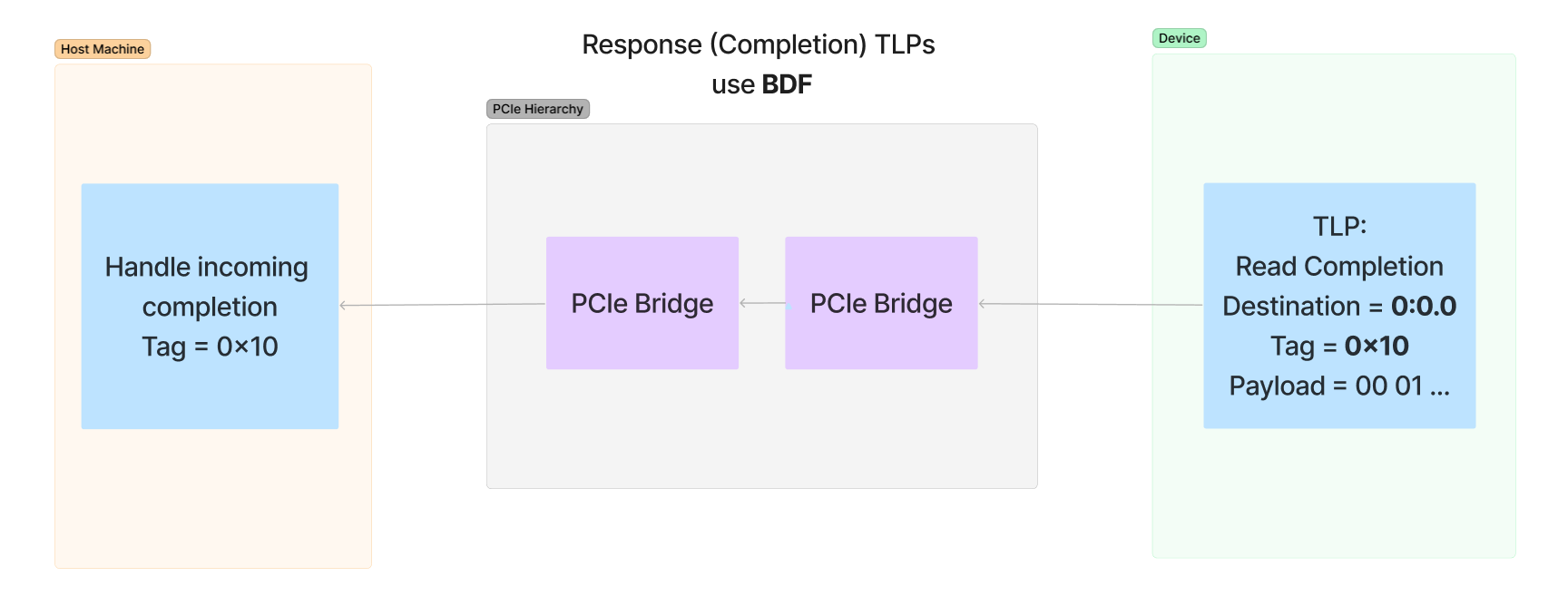
- The PCIe Bridges are in charge of translating Memroy Address to BDF
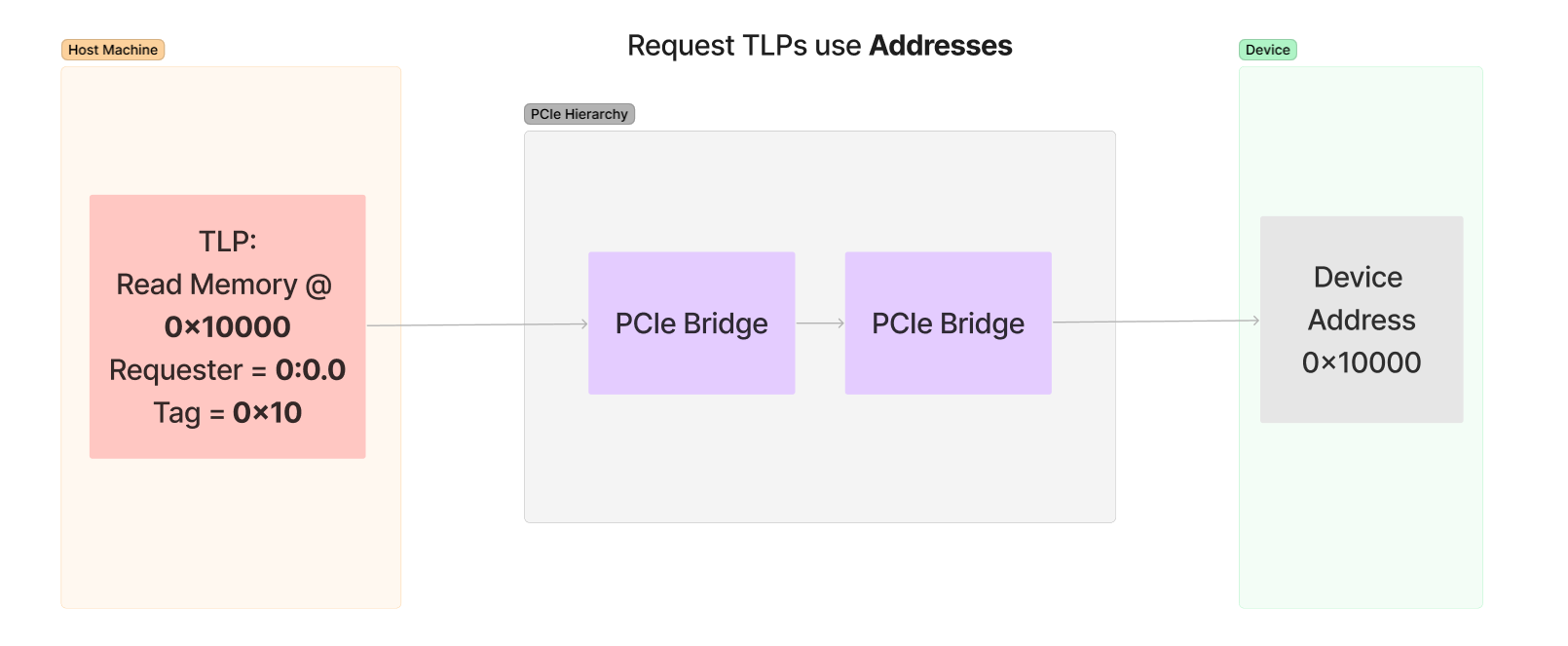
- The Memory Address used to detemine which device is being requested for access
DMA Engine
Reading Memory
- DMA Engine Creates TLP
- TLP Traverses Hierarchy - Root Complex
- DRAM Controller is Notified - Root Complex internally communicates with the DRAM controller
- Memory is Read from DRAM Response
- Memory is read from DRAM
- DRAM Controller Responds to Root Complex
- Root Complex Generates Completion
- DMA Engine receives TLP
- Target Memory is Written
- System is Interrupted (optional) - This gives the device driver a notification when the DMA has been successfully completed by the device.
This post is licensed under
CC BY 4.0
by the author.